TSMC is accelerating its panel‑level packaging development, focusing on the 310×310mm mainstream size and conducting glass substrate integration tests. The new packaging platform is named CoPoS (Chip on Panel on Substrate), with mass production targeted as early as 2028.
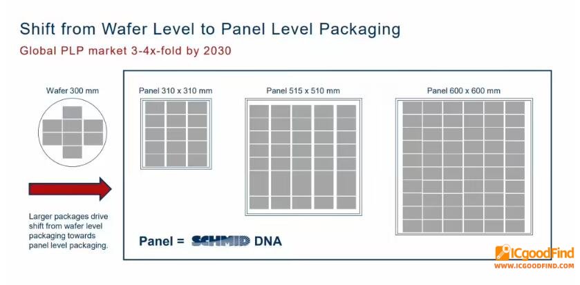
Unlike traditional round wafer packaging, panel‑level packaging uses a rectangular format and can replace silicon with glass substrates, reducing edge material loss and improving utilization. It breaks performance limits of organic substrates and silicon interposers, enabling higher integration density – widely seen as the next direction for advanced packaging.
Compared to today’s CoWoS, CoPoS offers larger area, better manufacturing efficiency, and lower cost. Technical challenges remain, including panel uniformity and warpage control.
Intel relies on partners like Ibiden and Unimicron for substrates rather than building its own lines. The industry expects CoPoS to start with small‑volume trials before ramping.
ICgoodFind: TSMC’s CoPoS aims to reshape advanced packaging with better scale and cost – a critical enabler for next‑gen high‑end chips.
